PVD 製程介紹
Vacuum Evaporation
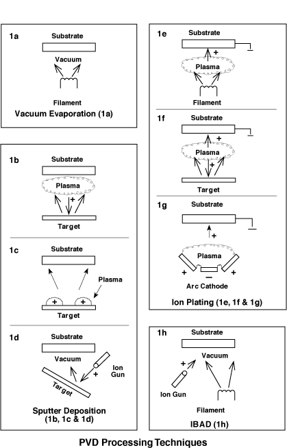
Vacuum evaporation is a PVD process in which material from a thermal vaporization source reaches the substrate without collision with gas molecules in the space between the source and substrate. The trajectory of the vaporized material is "line-of-sight". The vacuum environment also provides the ability to reduce gaseous contamination in the deposition system to a low level. Typically, vacuum evaporation takes place in the gas pressure range of 10 -5 Torr ** to 10-9 Torr depending on the level of gaseous contamination that can be tolerated in the resulting deposited film. The figure depicts a simple vacuum evaporation arrangement using a resistively-heated filament vapor ization source.
Advantages of vacuum evaporation high purity films can be deposited from high purity source material source of material to be deposited may be a solid in any form and purity the line-of-sight trajectory and "limited-area sources" allow the use of masks to define areas of deposition deposition monitoring and control are relatively easy probably the least expensive of the PVD processes
Disadvantages of vacuum evaporation many alloy compositions and compounds can only be deposited with difficulty line-of-sight and limited-area sources result in poor surface coverage on complex surfaces without proper substrate fixturing and movement line-of-sight trajectories and limited-area sources results in poor film thickness uniformity over large areas film properties depend on the "angle-of-incidence" of the flux of depositing material substrate fixturing with movement capability is necessary to improve surface coverage and thickness uniformity few processing variables are available for film property control source material utilization may be poor high radiant heat loads can exist in the deposition system
Vacuum evaporation is used to form optical interference coatings, mirror coatings, decorative coatings, permeation barrier films on flexible packaging materials, electrically conducting films, and corrosion protective coatings.
Sputter Deposition
Sputter deposition is the deposition of particles vaporized from a surface, which is
called the "sputtering target", by the physical sputtering process. Physical
sputtering is a non-thermal vaporization process where surface atoms are physically
ejected by momentum transfer from an energetic bombarding particle which is usually a
gaseous ion accelerated from a plasma. This PVD process is sometimes just called
sputtering i.e. "sputtered films of ____ " which is an improper term in that the
film is not being sputtered. Sputter deposition can be performed in a vacuum or low
pressure gas (<5 mTorr) where the sputtered particles do not suffer gas phase
collisions in the space between the target and the substrate or in a higher gas pressure
(5-30 mTorr) where energetic particles sputtered or reflected from the sputtering target
are "thermalized" by gas phase collisions before they reach the substrate
surface. The figure shows several sputter deposition configurations.
Advantages of sputter deposition elements, alloys and compounds can be sputtered and deposited the sputtering target provides a stable, long-lived vaporization source in some configurations the sputtering target provides a large-area vaporization source that can be of any shape in some configurations the sputtering source can be a defined shape such as a line or segment of a cone in some configurations reactive deposition can be easily accomplished using reactive gaseous species that are "activated" in a plasma (i.e. "reactive sputter deposition")
Disadvantages of sputter deposition sputtering rates are low compared to those that can be attained in thermal evaporation film properties depend on the "angle-of-incidence" of the flux of depositing material and at low pressures the amount of bombardment from high energy neutrals reflected from the sputtering target in many configurations the deposition flux distribution is non-uniform requiring fixturing to randomize the position of the substrates in order to obtain films of uniform thickness and properties sputtering targets are often expensive and material utilization may be poor most of the energy incident on the target turns into heat which must be removed in some configurations gaseous contamination is not easily removed from the system and gaseous contaminants are "activated" in the plasma thus making film contamination more of a problem than in vacuum evaporation in some configurations radiation and bombardment from the plasma or sputtering target can degrade the substrate
Sputter deposition is widely used to deposit thin film metallization on semiconductor material, coatings on architectural glass, reflective coatings on compact discs, magnetic films, dry film lubricants and decorative coatings.
Ion Plating
Ion plating utilizes concurrent or periodic energetic particle bombardment of the
depositing film to modify and control the composition and properties of the depositing
film. The depositing material may be vaporized either by evaporation, sputtering, arc
erosion or other vaporization source. The energetic particles used for bombardment are
usually ions of an inert or reactive gas, or ions of the depositing material ("film
ions"). Ion plating can be done in a plasma environment where ions for bombardment
are extracted from the plasma or it may be done in a vacuum environment where ions for
bombardment are formed in a separate "ion gun". The latter ion plating
configuration is often called Ion Beam Assisted Deposition (IBAD). The figure shows two
forms of ion plating in a plasma environment and ion plating in a vacuum environment or
IBAD.
Advantages of ion plating significant energy is introduced into the surface of the depositing film by the energetic particle bombardment surface coverage can be improved over vacuum evaporation and sputter deposition due to gas scattering and "sputtering/redeposition" effects controlled bombardment can be used to modify film properties such as adhesion, density, residual film stress, optical properties, etc. film properties are less dependent on the "angle-of-incidence" of the flux of depositing material than with sputter deposition and vacuum evaporation due to gas scattering, "sputtering/redeposition" and "atomic peening" effects bombardment can be used to improve the chemical composition of the film material by "bombardment enhanced chemical reactions" and sputtering of unreacted species from the growing surface in some applications the plasma can be used to "activate" reactive species, and create new chemical species that are more readily adsorbed so as to aid in the reactive deposition process ("reactive ion plating")
Disadvantages of ion plating there are many processing variables to control it is often difficult to obtain uniform ion bombardment over the substrate surface leading to film property variations over the surface substrate heating can be excessive under some conditions the bombarding gas may be incorporated into the growing film under some conditions excessive residual compressive film stress may be generated by the bombardment
Ion plating is used to deposit hard coatings of compound materials, adherent metal coatings, optical coatings with high densities, and conformal coatings on complex surfaces.
* Footnote: 1 nanometer (nm) = 10-9 meters = 10 Angstroms (A) = 10-3
microns = 0.04 microinches.
** Footnote: Standard atmospheric pressure = 760 mm mercury (or Torr) or 1.01 x 10⁵
Newtons per meter square (or Pascals). 1 Torr = 103 milliTorr (mTorr). 1 mTorr
= 7.5 Pascals (Pa) = 1 micron (of mercury)